Institut Charles Sadron SYCOMMOR
Research
TOPIC 1. Growth control and structure in (macro)molecular systems
TOPIC 2. Organogelators and p-conjugated self-assembled systems
TOPIC 3. Morphogenesis of hybrid systems
TOPIC 4. Influence of hydrogen-bonding in organic electronics. Use of diketopyrrolopyrrole as a model
TOPIC 5. Organic Thermoelectrics
TOPIC 1. Growth control and structure in (macro)molecular systems
The (opto)-electronic properties of organic semiconductor materials and particularly those of semiconductor polymers are essentially anisotropic. They are highly dependent on the orientation of polymer chains and thin film order and crystallinity. To control the growth and structure of these materials, the group has developed two main techniques: mechanical rubbing of films at high temperature and crystallization by epitaxy. This control makes it possible to highlight fundamental aspects of the crystallization and structure of polymers by TEM (High Resolution TEM and electron diffraction).
The principle of these techniques and examples of our work are described below.
A. Description of growth and alignment techniques
1. Orientation by "friction transfer".
This method is used to prepare aligned PTFE substrates. PTFE fibers are transferred by friction at controlled pressure and temperature to a unidirectional moving glass slide.
2. Crystallization by directional epitaxy in crystallizable solvent
This method allows very high rates of alignment and crystallinity of pi-conjugated materials to be obtained over small areas. It consists in crystallizing the sample from the molten state by moving it very slowly (few µm/s to µm/min) in a temperature gradient. The samples thus obtained are studied by TEM and electron diffraction and used in particular for the resolution of crystalline structures.
3. Mechanical rubbing of thin films at high temperature
The alignment of the polymer chains is done by shear force along the rubbing direction. This technique is compatible with large surfaces and all types of substrates. The temperature during film rubbing plays an important role in the degree of alignment of polymer chains. A new rubbing machine has recently been developed and transferred to the glove box system of ICube's organic electronic platform (UMR7357, Strasbourg). It is used in the development of high-performance organic electronic devices (OFETs, OLEDs, OLDs, Thermoelectricity).
B. Some examples of applications
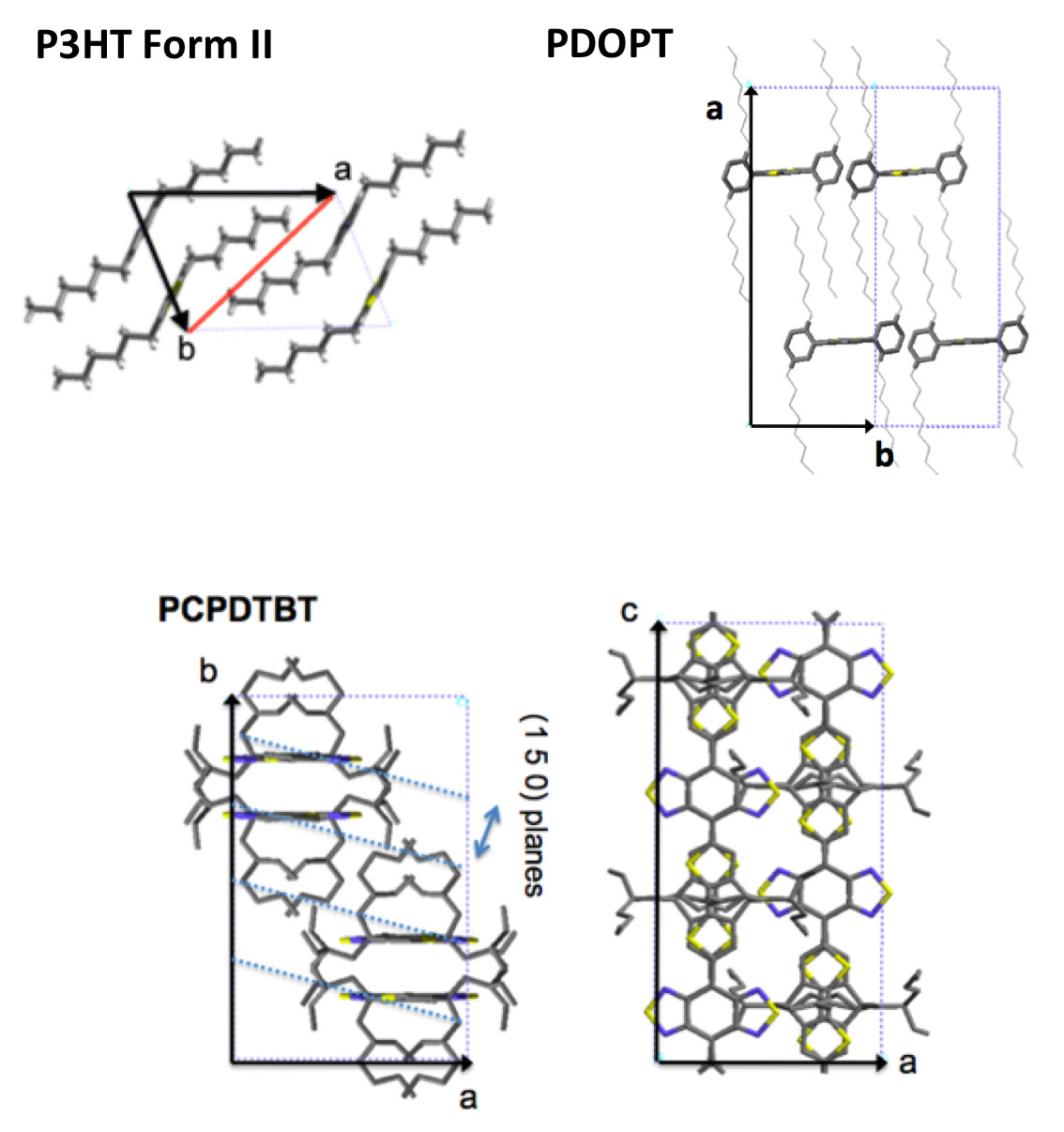
The thin films with controlled structure and orientation have made it possible to determine the structure of several semiconductor polymers most representative of the organic electronics field form I and form II of P3HT, PDOPT, PCPDTBT, p(NDI2OD-T2), F-PCPDTBT and PTB7... [1]
For P3HT, correlations between the length of planarized chain segments in crystals and optical properties (exciton bandwidth) and charge transport (hole mobility) were demonstrated for the first time.
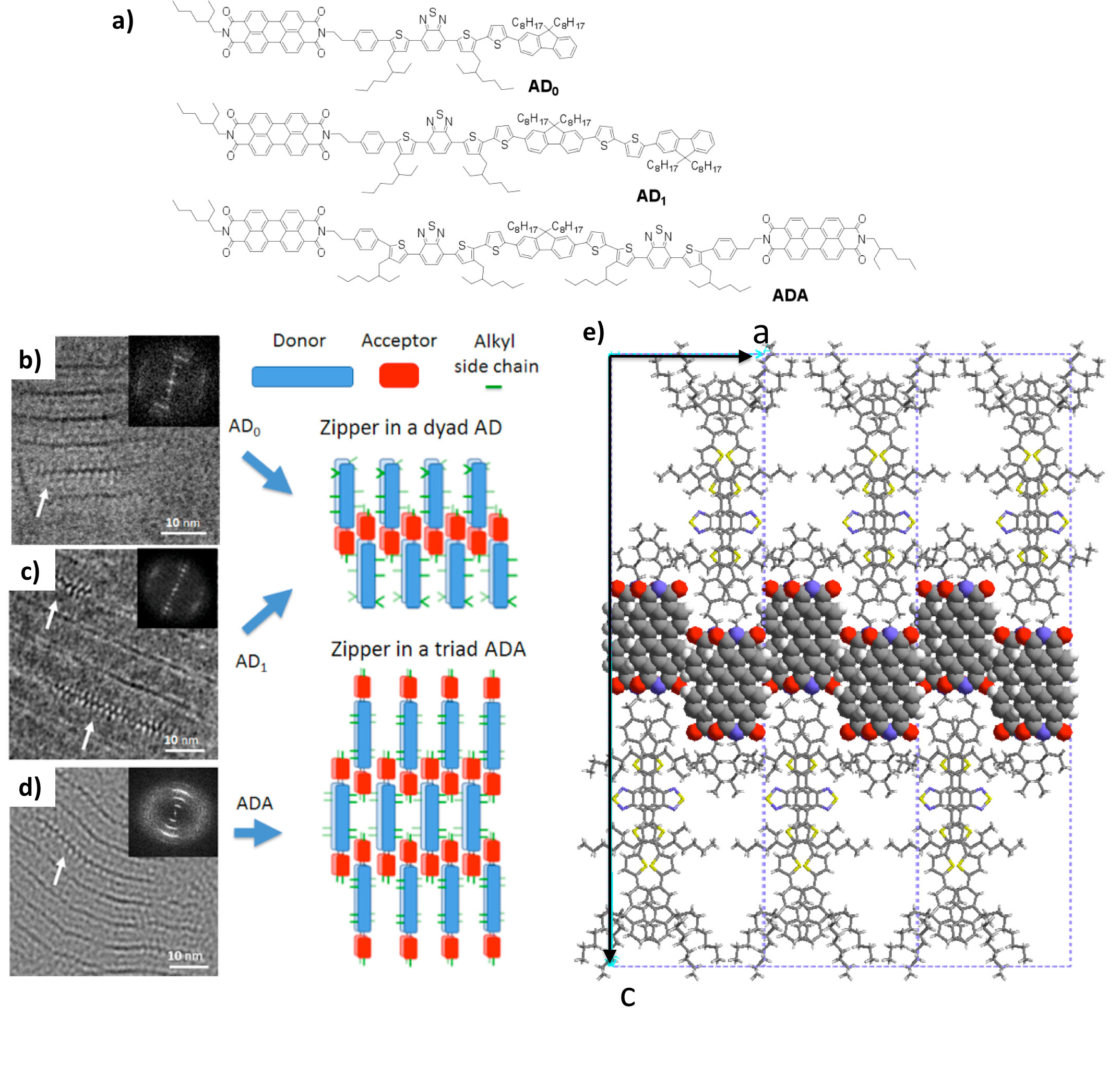
This approach has been successfully used to orient donor –acceptor bloc oligomeric lamellar mesophases designed for the development of single-component solar cells (ANR Picasso). HRTEM has identified a new zipper-like assembly of PDI molecules. The following figure illustrates the original structures of these co-oligomers obtained by electron diffraction analysis and structural modeling. [2]
References:
1. Structural Model of Regioregular Poly(3-hexylthiophene) Obtained by Electron Diffraction Analysis, N. Kayunkid, S. Uttiya, and M. Brinkmann, Macromolecules 2010, 43, 4961–4967.
Highly Crystalline Films of PCPDTBT with Branched Side Chains by Solvent Vapor Crystallization: Influence on Opto-Electronic Properties, F.S. U. Fischer, D. Trefz , J. Back, N. Kayunkid, B. Tornow ,S. Albrech , K. G. Yager, G. Singh, A. Karim , D. Neher, M. Brinkmann and S. Ludwigs
Highly oriented and crystalline films of a phenyl-substituted polythiophene prepared by epitaxy: structural model and influence of molecular weight, Hamidi - Sakr, A.; Schiefer, D.; Covindarassou, S.; Biniek, L.; Sommer, M.; Brinkmann, M., Macromolecules 2016, 49 (9), 3452–3462.
Structure and charge transport anisotropy of polythieno[3,4-b]-thiophene-co-benzodithiophene (PTB7) oriented by high-temperature rubbing, L. Biniek, A. Hamidi-Sakr, L. Grodd, S. Escoubas, Y. J. Dapp, S. Grigorian, M. Brinkmann Adv. Electron. Mater. 2018, 1700480.
2. Zipper-like molecular packing of donor-acceptor conjugated co-oligomers based on perylenediimide, L. Biniek, P.-O. Schwartz, E. Zaborova, B. Heinrich, N. Leclerc, S. Méry, M. Brinkmann, J. Mater. Chem. C 2015, 3, 3342-3349.
Perylenediimide-Based Donor-Acceptor Dyads and Triads: Impact of Molecular Architecture on Self-Assembling Properties, P.-O. Schwartz, L. Biniek, E. Zaborova, B. Heinrich, M. Brinkmann, N. Leclerc, and S. Me´ry J. Am. Chem. Soc. 2014, 136, 5981-5992.
TOPIC 2. Organogelators and p-conjugated self-assembled systems
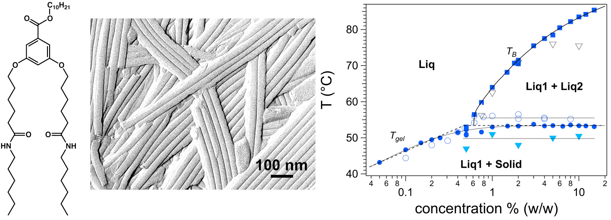
While a wealth of organogelators have been synthesized, their thermodynamics properties and the mechanisms of gelation in relation to the morphology/structure of the self-assemblies formed in solvents, are only marginally understood. In particular, establishing correlations between molecular structure of the gelating molecules and the shape/structure of the assemblies is an important issue. The group has shown that the interactions between esters in a series of analogue diamide-ester gelators are the most determining (see chemical structure in Fig.1.). The ester length controls the shape of the aggregates : flat ribbons, twisted ribbons or nanotubes and, in the last case, the diameter of the tubes. A second important contribution is the precise determination of a complete phase diagram for a model organogelator. The combination of DSC, rheology and OM, revealed the presence of a miscibility gap, underlining the inherent complexity of phase diagrams of organogelators. In the case of amino-acid gelators, a so-called “jamming” transition has been evidenced by rheological measurements to explain the gelation mechanism.[1]
Finally, the group investigated the structure formation in pi-conjugated semiconductors based on perylene-bisimide (PBI). The group has shown that a PBI organogelator behaves as a reversible stimuli responsive material (Thesis A. Sarbu). TEM and GIXD studies demonstrated that the property modification results from a structural reorganization from columnar to supramolecular helical assemblies. [2]
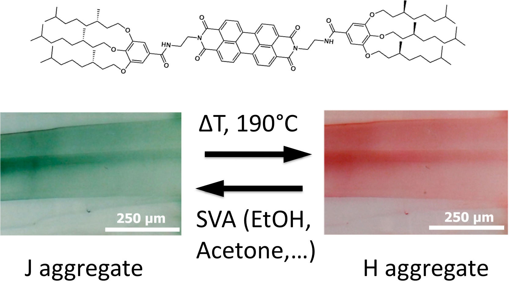
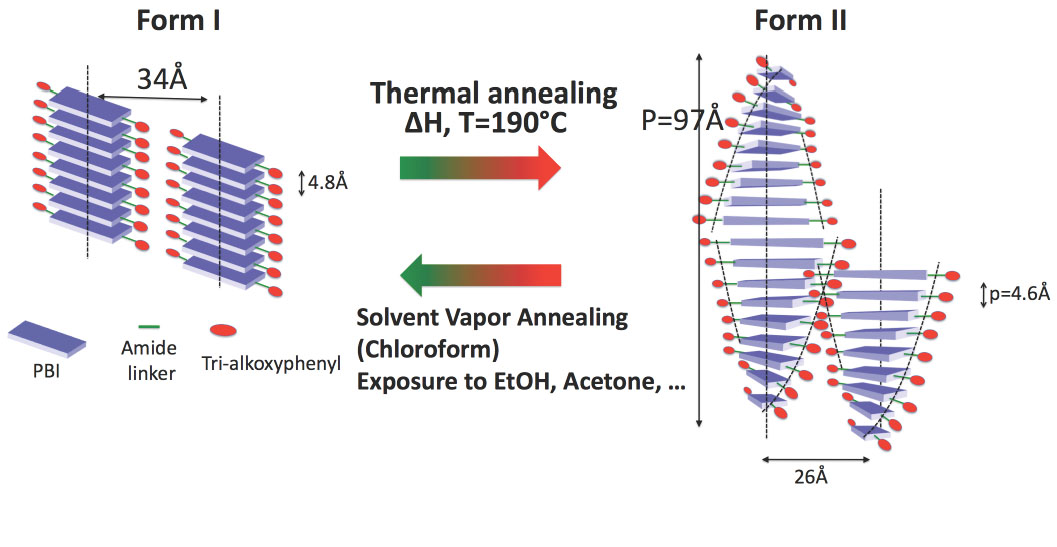
Fig.2. : Illustration of the structural reorganisation from a columnar to a helical stacking of a N,N’-substituted perylenebisimide organogelator, responsible for the change in optical absorption (form I : green and form II : red).
References:
1. N. M. Sangeetha, et al. ACS Nano, 2012.Simon, F.-X. ; et al. Soft Matter 2013. Collin, D. et al. Soft Matter, 2013. Christ, E. ; et al. Langmuir 2016.
2. A. Sarbu, et al. J. Mater. Chem.C, 2015.
A. Rheology and piezo-rheology of self-assembling systems
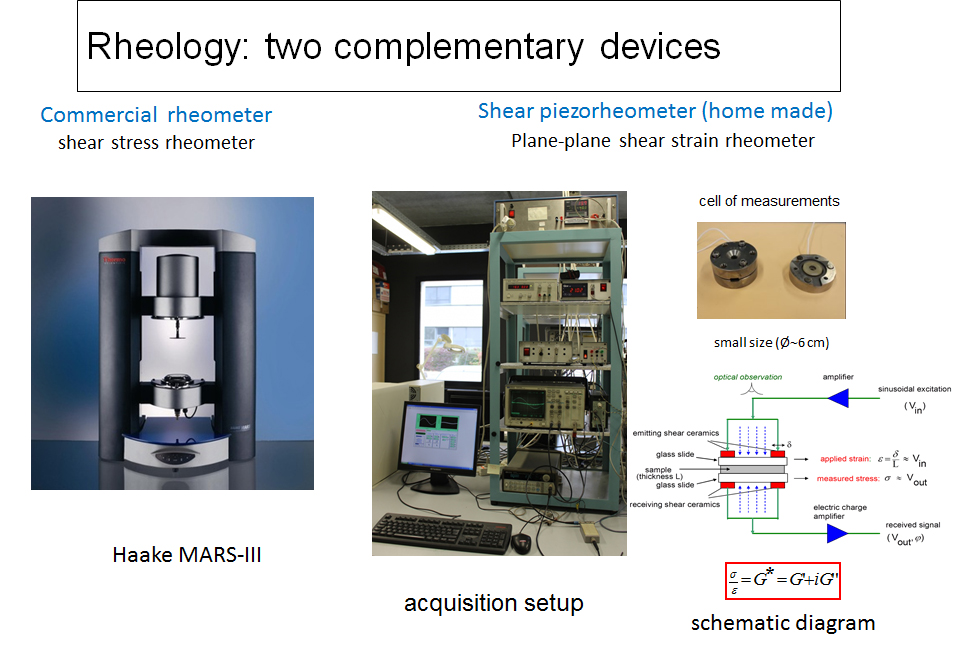
The characterization of the rheological properties of self-assembled systems involves the use of two complementary measuring devices: an imposed stress rheometer (Haake Mars III) and an imposed deformation piezorheometer operating with piezoelectric elements.
References:
- Divry, V. ; Gromer, A. ; Nassar, M. ; Lambourg, C. ; Collin, D. ; Holl, Y. Drying Mechanisms in Plasticized Latex Films. Role of Horizontal Drying Fronts. The Journal of Physical Chemistry B, 120, 6791, 2016.
- Christ, E. ; Blanc, C. ; Al Ouahabi, A. ; Maurin, D. ; Le Parc, R. ; Bantignies, J.-L. ; Guenet, J.-M. ; Collin, D. ; Mésini, P. J. Origin of Invariant Gel Melting Temperatures in the c-T Phase Diagram of an Organogel. Langmuir, 32, 4975, 2016.
- Aguilar, A. ; Pertuy, F. ; Eckly, A. ; Strassel, C. ; Collin, D. ; Gachet, C. ; Lanza, F. ; Léon, C. Importance of Environmental Stiffness for Megakaryocyte Differentiation and Proplatelet Formation. Blood , American Society of Hematology , 128, 2022, 2016.
Optical absorption measurements
The optical absorption of a sample is very sensitive to the appearance of diffusing objects (e. g. droplets). The measurement of this absorption, correlated with optical microscopy, makes it possible to accurately detect the existence of a heterogeneous homogeneous liquid-liquid phase separation, as in the case of diamid organogelator solutions (*).
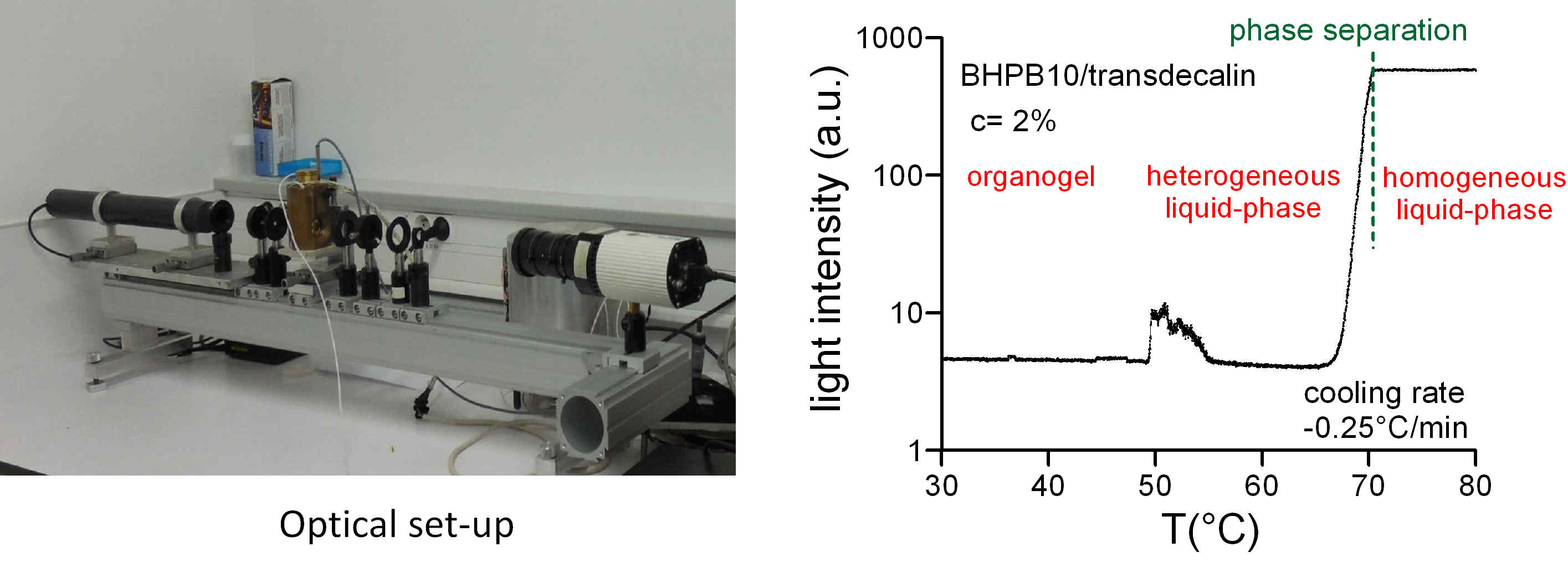
(*) Christ, E. ; Blanc, C. ; Al Ouahabi, A. ; Maurin, D. ; Le Parc, R. ; Bantignies, J.-L. ; Guenet, J.-M. ; Collin, D. ; Mésini, P. J. Origin of Invariant Gel Melting Temperatures in the c-T Phase Diagram of an Organogel. Langmuir, 32, 4975, 2016.
TOPIC 3. Morphogenesis of hybrid systems
The group has investigated the morphogenesis of hybrid functional materials using physico-chemical methods (heterogeneous nucleation, physical gelation). The hybrid materials investigated by the group combine self-assembled molecules (SAM) and polymers with complementary properties (electron-donor and –acceptor properties or insulating and semi-conducting properties). Nanofibers of perylenebisimide-organogelators used as nucleating agents of PSCs produced shish-kebab nanostructures (thesis Région Alsace, A. Sarbu). The superhelical structure of a fluorinated organogel BHPBF was observed to coil around sPS fibrils by a mechanism of heterogeneous nucleation.
Nano-cables were formed by sheathing polymer semi-conductor nanofibrils with insulating nanotubes (ANR MATISSE) (sheathing was proved by neutron scattering and C-AFM) (Coll. SprAM Grenoble, L3C, Montpellier). Filaments of copper complexes were sheathed with polymer fibrils, which modified their intrinsic magnetic properties.
Within the EU project HYMEC, the group developed also growth methods to prepare highly organized/oriented nanostructured hybrids made of organic semiconductors and inorganic nanoparticles (Au and Ag, CdSe), of interest for hybrid non volatile memories. TEM (tomography, diffraction) helped understand the mechanisms of metal diffusion and metal nanoparticle growth on various (macro)molecular semi-conductors (Coll. Humbolt Uni. Berlin, Univ. Namur, Univ. Lodz, Uni. Tübingen).
• Making of polymer/self-assembled system hybrid materials
We have developed the making and characterization of new molecular architectures consisting of covalent polymers and functional fibrillar organogels [1-4]. As a rule, these organogels cannot be processed into materials on account of their poor mechanical properties as their fibrillar structure is chiefly obtained at rather low concentrations. The use of a covalent polymer matrix can be an appropriate choice for retaining the original organogel fibrillar structure while allowing a better tractability of the system. The originality of our approach consists in using thermoreversible gels of co-valent polymers together with physical processes for achieving the fine, mesoscopic dispersion of the orga¬nogels into the polymer network. This is made possible because these covalent polymer gels also possess a similar fibrillar morphology, particularly an average mesh size in the micrometer range. While these novel molecular architectures may be relevant for applications in functional materials the primary goal of these investigations is to establish a proof of concept.
Two types of systems have been considered : intermingled gels where the organogel grows within the polymer gel with little perturbation ; and “sheathed” fibrils where nanotubes encapsulate polymer gel fibrils.
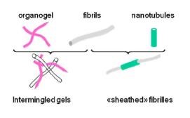
Figure 1 : Sketch of the two types of hybrid systems.
• Intermingled gels of stereoregular polystyrenes and oligo phenylene vinylene organogels.
The feasibility of intermingled gels has been investigated as a function of polymer, organogel concentration and temperature, by differential scanning calorimetry (DSC), optical microscopy, and AFM [2]. The organogel was made up from p-conjugated oligo (phenylene vinylene) (OPVOH) while the polymer gel was prepared from isotactic polystyrene (iPS) or syndiotactic polystyrene (sPS). OPV organogels change colour at the SOL-GEL transition (yellow to green).
We have observed that a mesoscopic dispersion of one gel into another could be achieved [1-2] provided the mesh size of either gel is in the micrometer range (see Figure 2). For smaller mesh size, microscopic phase separation occurs. These results were confirmed by SAXS and SANS. Basically, we can keep the organogel concentration rather low (0.004 g/cm3), and so retaining the optical property while increasing dramatically the elastic modulus of the ternary gel. This process is totally reversible as the organogel can be melted and then reformed by cooling without altering the polymer gel structure.
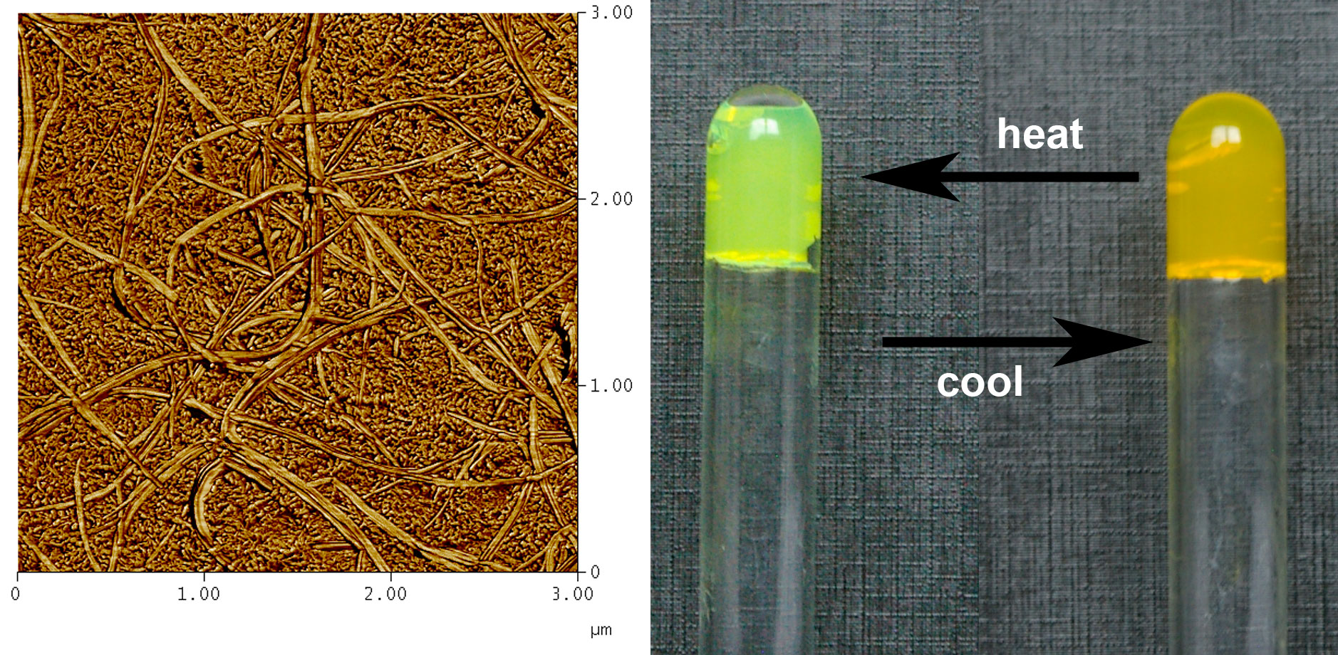
Figure 2 : left AFM image of an intermingled gel [1]. Organogel= large cross-section fibrils, polymer gel= small cross-section fibrils; right the melting of the organogel can be achieved without altering the polymer gel, hence a change of colour without change of the mechanical properties.
• Intermingled gels between PVC and oligo phenylene vinylene organogels.
The making of hybrid materials from polymers and self-assembled systems may open up new horizon for imparting new properties to usual polymers without recourse to chemistry. Here it is again shown that preparation of intermingled gels can be straightforwardly achieved by a physical SOL-GEL process with polyvinyl chloride (PVC), an extensively-used polymer, and oligo(p-phenylenevinylene) organogelators (OPVOH) [5]. Low amounts of OPV with respect to PVC are used (ratio ~1/10 to ~1/30). Although the PVC structures form first, the thermodynamic of the OPVOH gelation is virtually not altered (same formation temperatures and same melting temperatures). It is observed that the organogel does pervade the polymer structures, which results in a noticeable strengthening of the mechanical properties (figure 3).
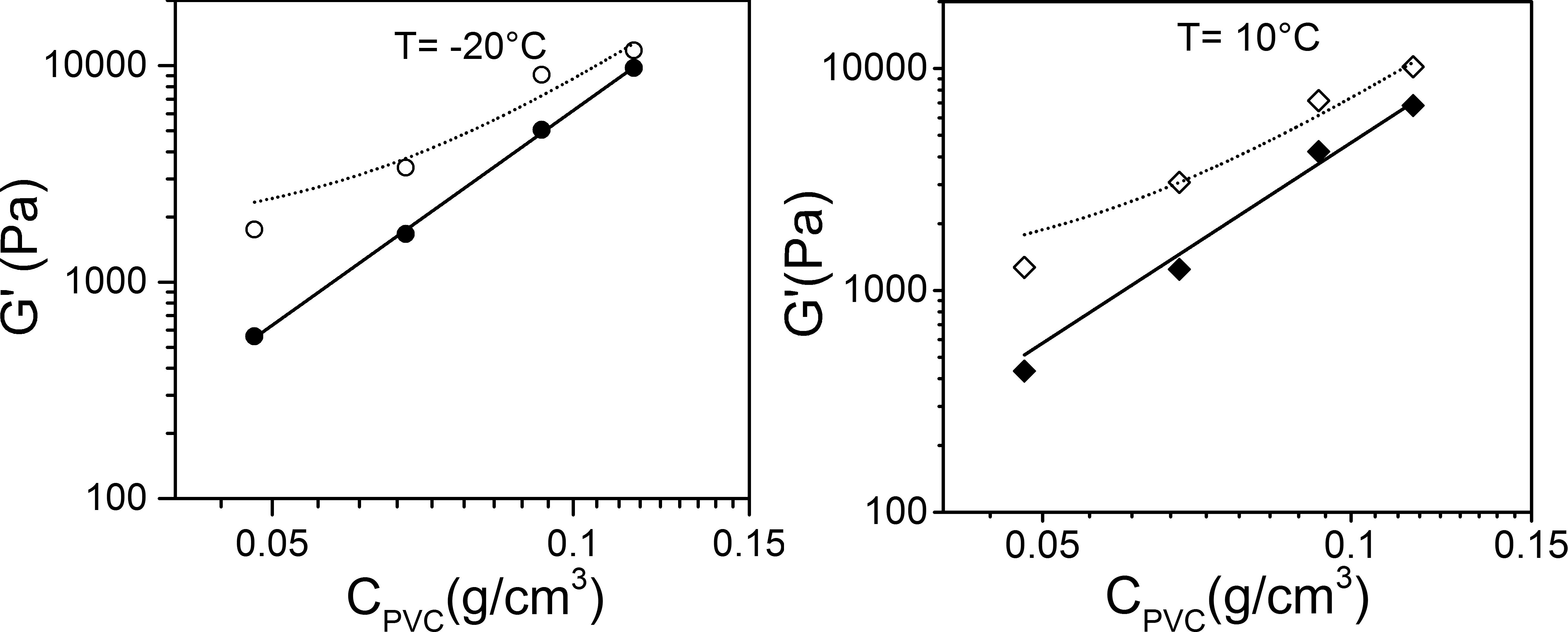
Figure 3: Variation of the elastic modulus G’ as determined at frequency= 1Hz and at T= -20°C (left) and T= 10°C (right) for PVC/bromobenzene gels (black symbols) and PVC/OPVOH16/bromobenzene gels (open symbols) [5].
• Sheated polymer fibrils by nanotubes.
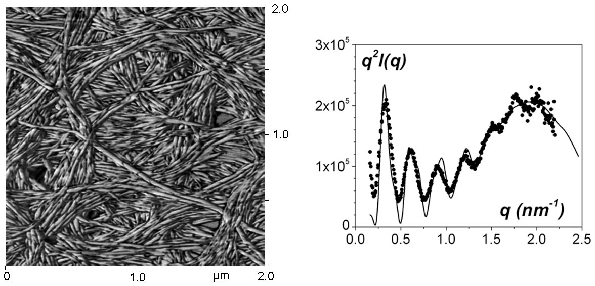
Figure 4 : left : AFM image of an array of nanotubules. The formation of the nanotubules arises from the wrapping of ribbons, which produces this ringlets aspect. ; right : SAXS curve with a fit obtained by considering a hollow cylinder and a structure maximum.[7]
Sheathing polymer fibrils, namely encapsulation of polymer gel fibrils by nanotubes (synthesis by P. Mésini [6] see figure 4 left) has been investigated by DSC, AFM and scattering techniques, SANS and SAXS. These nanotubules are of very low size polydispersity as oscillations are observed in the scattering curve that can be assigned to the scattering by a hollow cylinder.
We have observed by DSC that the formation exotherm and the melting endotherm of the nanotubes vanished when incorporated in a ternary system with iPS. Although the nanotube structure was still present in the ternary gel as ascertained by SANS, their formation was clearly concurrent with the polymer gel formation. We have concluded that nanotube formation is nucleated by iPS gel fibrils. AFM experiments have shown that the iPS fibril cross-section increased under these conditions, which is consistent with a sheathing process. SANS experiments have shown that only those fibrils with a diameter in register with the inner diameter of the nanotubes are sheathed [7].
This sheathing process is a low-energy path for physically modifying fibrils surface. This may have applications whenever finely dispersed media are required (e.g. catalysis, filtering membranes for capture of pollutants at the molecular level,.).
• Encapsulating self-assembled filaments in polymer fibrils
The bicopper complex molecule shown in figures 4 left possesses the propensity of self-assembling in organic solvent, thus generating very long filaments containing only one molecule in their cross-section [8-10]. The bicopper molecule is antiferromagnetic in the bulk state as described by the Bleaney-Bowers relation (figure 5 right).
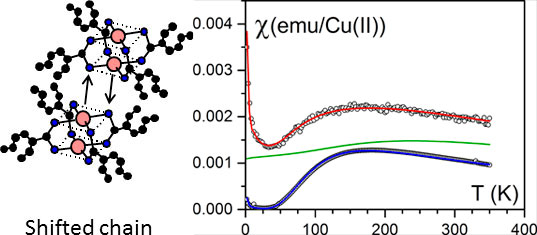
Figure 5. (left) the way the bicopper molecules pile up in the bulk state (shifted chains). (right) the magnetic susceptibility as a function of temperature. Blue= bulk state fitted with a Bleaney-Bowers law red= encapsulated state, green theoretical variation for a pure spin chain.

Figure 6. (left) Small-angle neutron scattering data for IPS/CuS8/trans-decahydronaphthalene gels: in all cases CiPS = 0.04 g/cm3, black dots for CCuS8 = 0.038 g/cm3, open dots for CCuS8 = 0.055 g/cm3. The solid lines (red and blue) are fit with theoretical models [8-9]. (right) sketch of the molecular structures for CCuS8 = 0.055 g/cm3: encapsulated fibrils, free associated filaments and their junctions. The encapsulated fibrils represent 99% of the structures.
Although the 1-D aspect of the filaments might be of interest for testing their magnetic properties, their instability with time together with the impossibility of keeping them apart after solvent removal made this a remote option. Alternatively, encapsulation of the bicopper filaments into polymer gel fibrils allows them to have an infinite life and to be kept apart so as to preserve their 1-D structure. This is achieved by a heterogeneous nucleation process, since the filaments act as an impurity towards the polymer, and so trigger the growth of the fibrils. Neutron scattering experiments have demonstrated that the polymer fibrils do encapsulate the bicopper complex filaments [9-10] (figure 6).
As shown in figure 5 right the magneric behaviour differs dratically whether the bicopper complex is in the bulk state or encapsulated.EXAFS investigations (Extended X-Ray Absorption Fine Structure) were performed for determining the environment of the copper atoms. The experimental results conspicuously differ in the encapsulated state. Cu-0 interactions between adjecent molecules are replaced by Cu-Cu interactions (figure 7 left) [9]. Thus, the encapsulated filaments are no longer purely shifted chains (figure 4 left) but certainly contain spin chains (figure 7 right).
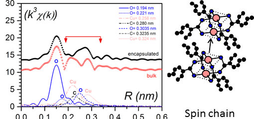
Figure 7. (left) Pseudo-radial distribution function in the vicinity of copper atoms as obtained by EXAFS; black dots for the encapsulated bicopper complex, red open circles for the bulk state (note there always is a difference of about 0.05 nm in EXAFS with the actual distances). The difference between the curves lies in the domain involving Cu-Cu distances; (right) a spin chain where there Cu-Cu interaction between adjacent molecules occur in lieu of the Cu-O interaction seen in the bulk state [10].
• Case of P3BT (Poly[3-butylthiophene-2,5-diyl]): a semi-conducting polymer sheathed by nanotubes.
Fibrils of P3BT (Poly[3-butylthiophene-2,5-diyl] figure 8 left) which is well-known in the organic electronics as p-type materials, have been sheathed by organic nanotubes as those shown above (bhpb-10, figure 4) again by means of a heterogeneous nucleation process [11].
As P3BT fibril grow somewhat slowly, the preparation procedure of the hybrid system involves three steps: first, the P3BT fibres are allowed to grow for several hours at room temperature, second the system is heated up at 60°C and then a bhpb-10 solution is added at the same temperature (no nanotubes are formed at this temperature), third the mixture is cooled down to room temperature for triggering the formation of nanotubes. The P3BT fibrils act there as impurities

Figure 8. (a) chemical structure of P3BT. (b) right: the tip of the C-AFM is gradually allowed to penetrate into the selected fibril until it reaches the gold layer. The current and the force are simultaneously measured to determine the conductivity and the penetration depth, respectively (for details see reference [11]).
The principle of C-AFM is shown in figure 8 right. Once a supposedly-sheathed fibril is spotted, the tip of the C-AFM is allowed to penetrate gradually into it while the current is measured (intensity vs voltage, I-V curve). The distance Z after the “jump to contact" is the sum of cantilever deflection and of the tip penetration/indentation depth (see figure 8 right).
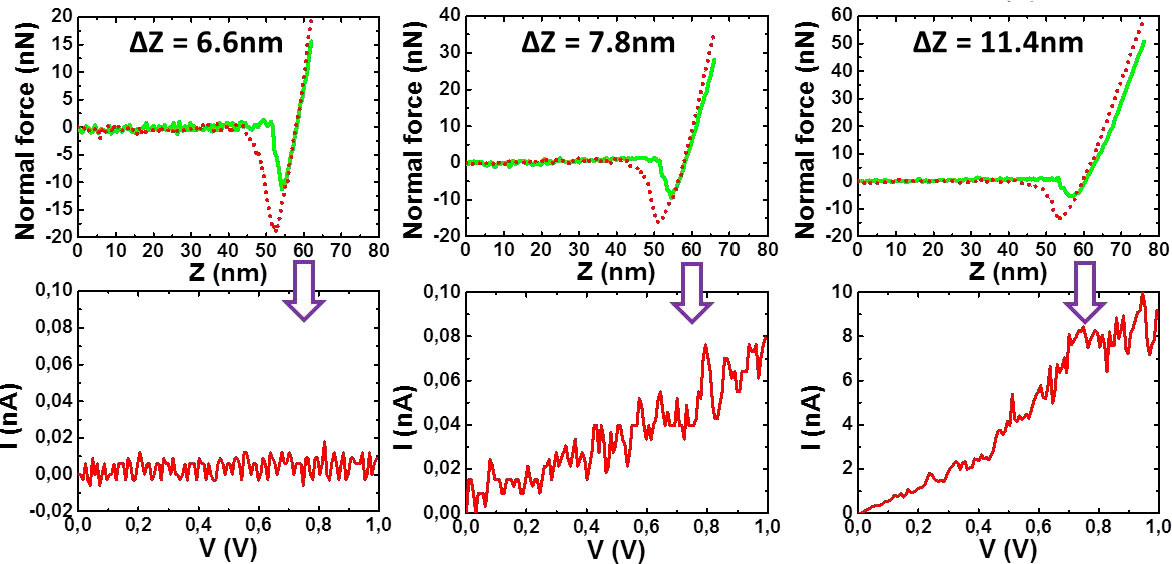
Figure 9. I-V plots (lower curves) vs penetration depth (upper curves). From left to right: insulator behaviour, appearance of current, semi-condutor behaviour. [10].
Figure 9 shows that the tip first encounters an isolating layer until it reaches a certain depth where the I-V curve corresponds to a semi-conducting system. This result gives a strong indication of P3BT fibrils being sheathed by bhpb-10 nanotubes. SANS experiments further back up these conclusions.
• Case syndiotactic polystyrene with a partially-fluorinated self-assembled system.
Another system involving a partially-fluorinated bhpb-10 (designated as bhpbf, see figure 10 right) and syndiotactic polystyrene (sPS) was investigated by Khan et al. with the aim of preparing highly hydrophobic materials. While the expected target was not reached, nanohybrid materials were still obtained [12]. As shown by neutron scattering (figure 10 left), bhpbf does not form nanotubes but twisted helices instead where the fluorinated moiety is located in their core (see figure 10 right). As a result, the bhpbf winds around the polymer fibrils. The polymer fibrils are therefore not carpeted by the bhpbf molecules.
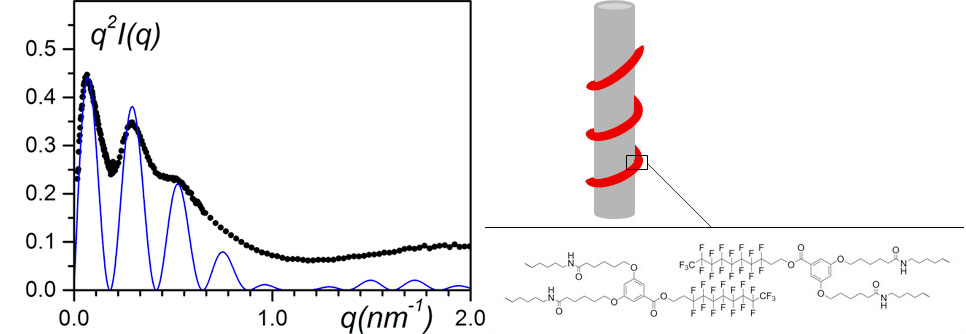
Figure 10. (left) SANS data plotted by means of a Kratky-plot, q2I(q) vs q.; black dots= sPSD/bhpbfH/o-xyleneD (CbhpbfH = 0.01 g/cm3, CsPSD = 0.15 g/cm3); solid line= fit with equation (9). (right) model designated as “bindweed”, where bhpbf irregular helices wind up around polymer fibrils [12].
[1] J.-M. Guenet
Nouveaux types de matériaux hybrides : polymère/système auto-assemblé
Matériaux et Techniques 2011 98, 329
Organogels: thermodynamics, structure, solvent role and properties 2016 Springer, N.Y.
[2] D. Dasgupta, S. Srinivasan, C. Rochas, A. Ajayaghosh, J. M. Guenet
Hybrid thermoreversible gels from covalent polymers and organogels -Langmuir 2009 25 8593
[3] D. Dasgupta, S. Srinivasan, C. Rochas, A. Thierry, A. Schröder, A. Ajayaghosh, J. M. Guenet
Insight into the gelation habit of oligo(para-phenylene vinylene) derivatives : effect of end-groups
Soft Matter, 2011, 7, 2797
[4] D. Dasgupta, S. Srinivasan, C. Rochas, A. Ajayaghosh, J.M. Guenet
Solvent-mediated fiber growth in organogels
Soft Matter 2011, 7, 9311.
[5] Z. Zoukal, S. Elhasri, A. Carvalho, M. Schmutz, D. Collin, P.K. Vakayil, A. Ajayaghosh, J.M. Guenet
Hybrid materials from poly[vinyl chloride] and organogels
ACS Applied Polymer Materials, 2019, 1, 1203
[6] N. Díaz, F.-X. Simon, M. Schmutz, M. Rawiso, G. Decher, J. Jestin and P. Mésini
Self-Assembled Diamide Nanotubes in Organic Solvents.
Angew. Chem., Int. Ed. Engl. 2005, 44, 3260
[7] D. Dasgupta, Z. Kamar, C. Rochas, M. Dahmani, Ph. Mésini, J.M. Guenet
Design of hybrid networks by sheathing polymer fibrils with self-assembled nanotubules
Soft Matter 2010 6 3576
[8] Terech, P.; Schaffhauser, V.; Maldivi, P.; Guenet, J. M.
Rheological and neutron scattering investigations of the jelly state of binuclear copper complexes in cyclohexane
Europhys. Let. 1992, 17, 515-521
[9] Lopez, D.; Guenet, J.M.
Encapsulation of filaments of a self-assembling bicopper complex in polymer nanowires. European Phys. J. B 1999, B12, 405-411
[10] Boulaoued, A. ; Bantignies, J.L.; Le Parc, R. ; Goze-Bac, C. ; Mesini, P. ; Nguyen, T.T.T. ; Al Ouahabi, A. ; Lutz, P. ; Guenet, J.M.
Hybrid fibrillar xerogel with unusual magnetic properties
Langmuir 2016, 32, 13193-13199
[11] Raj, G.; Boulaoued, A.; Lacava, J.; Biniek, L.; Mésini, P.J.; Brinkmann, M.; Faure-Vincent, J.; Guenet, J.-M.
Insulated Molecular Wires: Sheathing Semiconducting Polymers with Organic Nanotubes through heterogeneous Nucleation
Adv. Electron. Mater. 2017, 3, 1600370
[12] Khan, A.N.; Schmutz, M.; Lacava, J.; Al Ouahabi, A.; Nguyen, T.T.T.; Mesini, P.J.; Guenet, J.-M.
Design of Nanohybrid Systems from a Partially Fluorinated Organogelator and Syndiotactic Polystyrene thermoreversible Gel
Langmuir 2015, 31, 7666
TOPIC 4. Influence of hydrogen-bonding in organic electronics. Use of diketopyrrolopyrrole as a model
A. Systematic study using thiophene-capped DPP H-bonded derivatives
Supramolecular chemistry uses the power of noncovalent interactions among many individual species to achieve very precise structures with properties and functions not present when such species are isolated. Hydrogen bonds (H-bonds) are one of the noncovalent interactions employed to direct supramolecular assemblies into directional and well-organized structures. H-bonds are sensitive to temperature, solvent, concentration and chirality among other parameters, being possible to tune the aggregation state by varying any of them. This is very useful to program molecules to form the appropriate structures that will present specific properties and functions. This is the case of hydrogen-bonded semiconductors, where not only the electronic properties play an important role in the final outcome. The molecular packing and aggregation in solution and on thin film are equally important, making possible to influence the optoelectronic properties upon self-assembly. Diketopyrrolopyrrole (DPP) dyes are among the best electroactive segments used in semiconductors, since their discovery by Farnum in the 70’s while trying to synthesize azetinone, DPP has been one of the most used pigments in industrial applications and in the search of new materials. Multiple examples of polymers and small molecules can be found for the fabrication of organic solar cells, organic field effect transistors, and sensors. The optoelectronic properties of this molecule arise from its conjugated core and the functionalization in the 3- and 6- positions, being thiophene, phenyl and furan the main aromatic moieties used. Subsequently, further functionalization can be added according to the specific needs and the desired applications. For instance, electron-withdrawing or electron-donating groups can be introduced or the conjugation can be further extended using a push-pull strategy. A different way of achieving the properties wanted is by tuning the aggregation state of DPP using other noncovalent interactions, such as H-bonds, in combination with the present ?-? stacking. DPPs are considered H-bonded pigments due to the presence of unsubstituted amides in their structure. Such groups are normally alkylated to provide solubility and hence, unavailable to form H-bonds. However, H-bonding groups can be introduced in different parts of the DPP molecule, like in the periphery of the aromatic rings usually attached to the central core or even as a part of the solubilizing tails pending from the amide groups.
Our research is focused on making a systematic study of the influence of H-bonds using DPP as a model. Several parameters are being studied (Figure 1), including the H-bonding position, function and number of H-bonds, solubility and chirality.
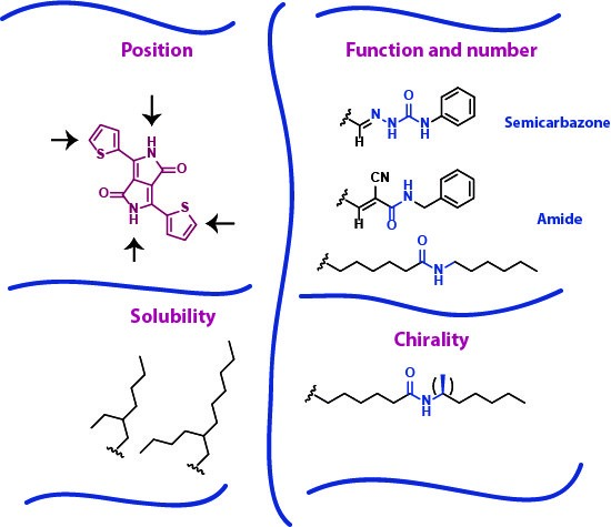
DPP derivatives based on semicarbazone and others containing amide bonds have been synthesized and their optoelectronic properties are being studied according to the aggregation state. UV-Vis, FTIR and circular dichroism (CD) spectroscopy are used for these studies, together with different microscopy techniques.
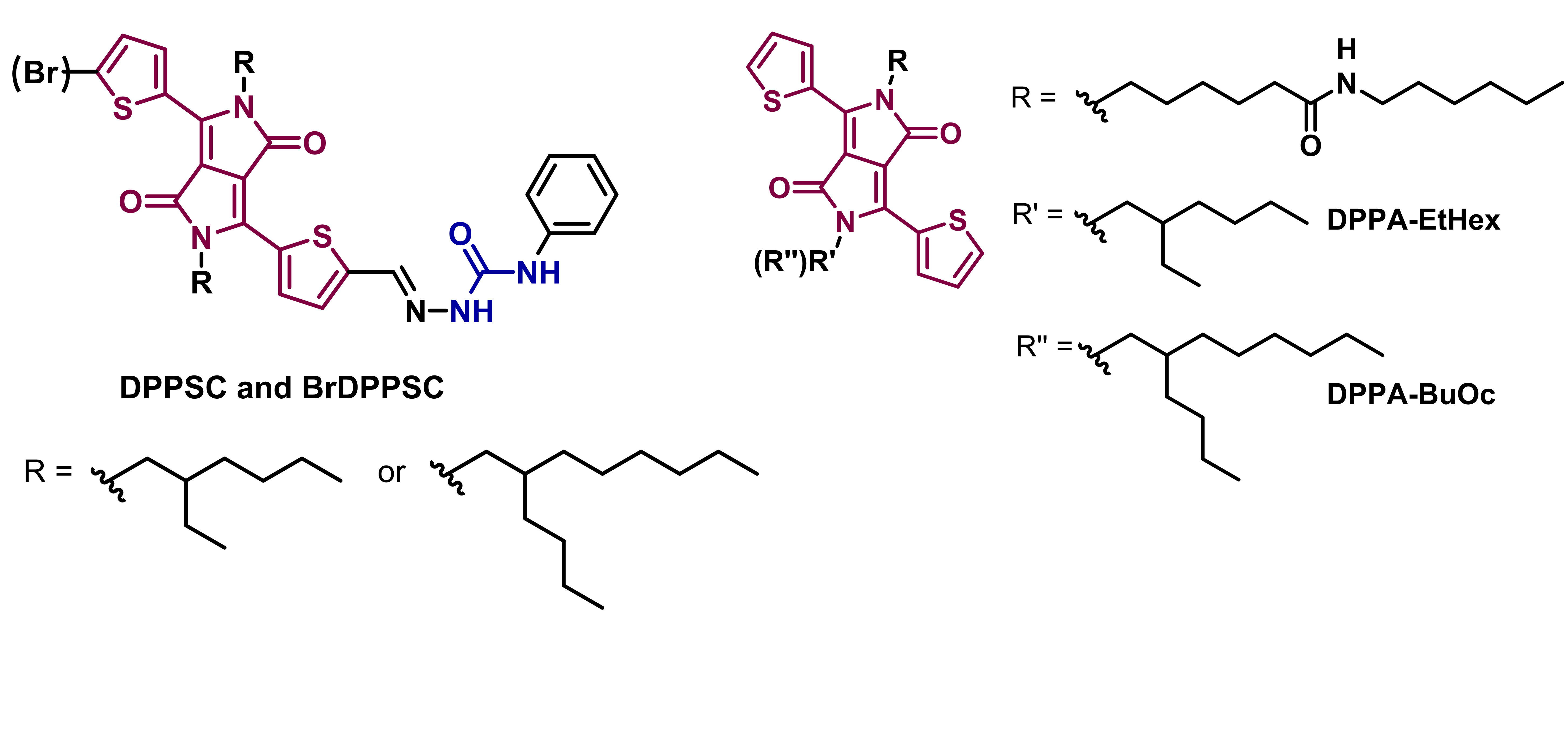
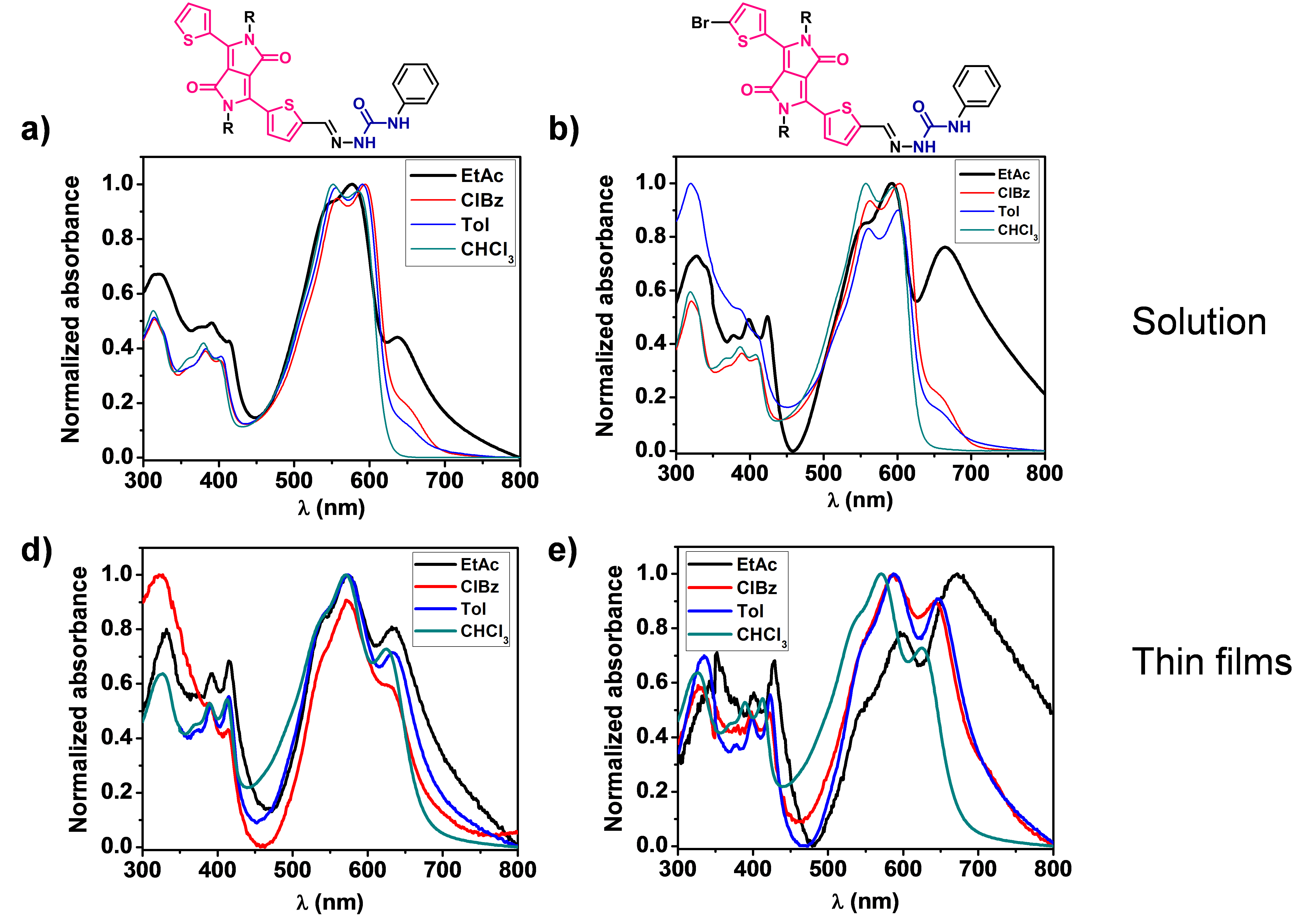
The formation of hydrogen bonds resulted in the appearance of J-aggregates, being possible to tune the bandgap and cover larger regions of the solar spectrum by modifying the aggregation state with different solvents, concentrations, temperature or the addition of hydrogen-bonding disrupting solvents (Figure 3).
Currently, the charge transport properties of all the H-bonded DPP derivatives synthesized are being measured at the University of Kyoto in collaboration with the group of Prof. Shu Seki. They are using flash-photolysis time resolved microwave conductivity to help us screening all the parameters we are currently studying.
References
S. Millitzer, T. M. P. Tran, P. J. Mesini, A. Ruiz-Carretero. ChemNanoMat. 2018, 8, 790-795.
B. Real time morphology studies
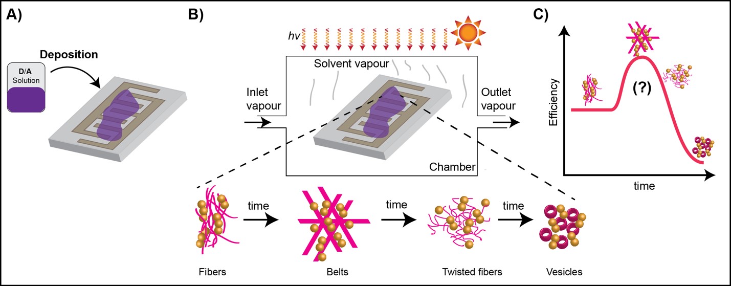
In order to facilitate the systematic study of the H-bonded DPP derivatives, we are working on the fabrication of a setup where changes in morphology can be measured in real time while testing devices. Solvent vapor will be applied in a controlled manner in a chamber where a substrate based on co-planar capacitators will have a thin film of the material to be studied.
TOPIC 5. Organic Thermoelectrics
The SYCOMMOR team is developing a new and very simple method for manufacturing conductive polymer films that amplifies the thermoelectric properties.
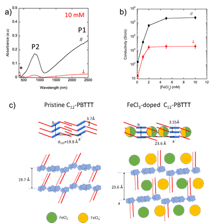
The polymer chains are first oriented and crystallized using the high temperature rubbing technique (Fig1 a). Then, by simple chemical doping, the polymer layers initially semiconducting are transformed into perfectly oriented and highly crystalline conductive layers. The team is interested in the structure - property relationships of these anisotropic polymer layers. The thermoelectric properties of these polymers make it possible to generate a voltage, and therefore an electric current by the so-called "Seebeck" effect, when two metal/polymer junctions are placed at different temperatures. The study of the charge transport and thermoelectric properties of these layers shows a significant increase in conductivity and the "Seebeck" effect in the direction of polymer chains induced by rubbing (Fig1 d).1,2
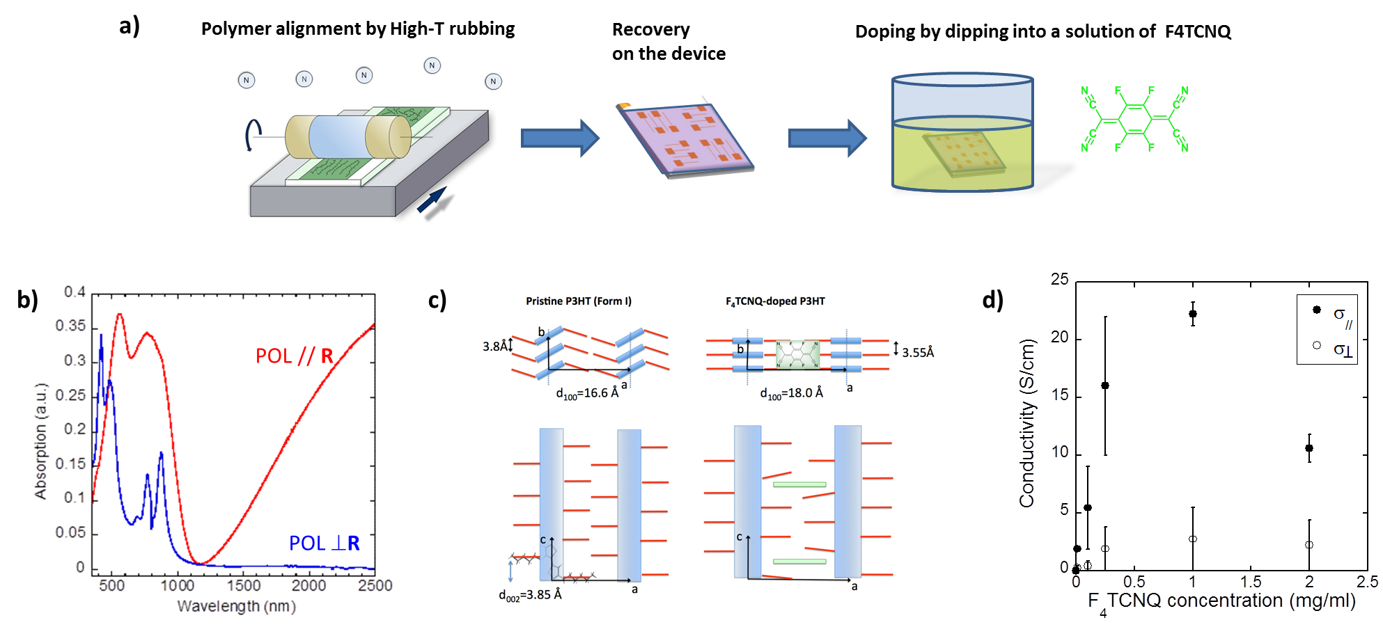
Central to this approach is the preservation of high order present in the pristine polymer semiconductors upon doping. This is possible when the dopants intercalate progressively into the layers of side chains by incremental increase of the dopant concentration. In this way, dopant intercalation preserves orientation and pi-stacking of the conjugated polymer backbones.
Our recent results break a thirty-year old record in terms of charge conductivity and thermoelectric power factor (obtained at that time for iodine-doped oriented polyacetylene (PA), systems that are very difficult to process because of the poor solubility of PA). We demonstrated that FeCl3 doping of highly crystalline and aligned films of C12-PBTTT results in charge conductivities up to 2.105 S/cm and metallic-like thermopowers. The conductivity is highly anisotropic (fig 2b) and the polaronic bands are strongly polarized along the polymer backbone (fig 2a).The combination of TEM, ED and Polarized absorption spectroscopy studies of such highly doped films provides important information on the structure. Variation of the polymer structure upon doping is illustrated in Fig 2c.
Thus, this new approach makes it possible to improve the power factor of these thermoelectric polymer films by taking advantage of their anisotropic properties and demonstrate the high potential of conducting polymers for flexible electronic. These outstanding results also show that this efficient, fast and low-cost manufacturing method could be applied to many semiconducting polymers.
References:
1."A versatile method to fabricate highly in-plane aligned conducting polymer films with anisotropic charge transport and thermoelectric properties: Key role of alkyl side chain layers on the doping mechanism". A. Hamidi-Sakr, L. Biniek, J.-L. Bantignies, D. Maurin, L. Herrmann, P. Algayer, N. Leclerc, V. Vijayakumar, N. Zimmermann, P. Lévêque, M. Brinkmann, Adv. Funct. Mat. 2017, 1700173.
2.“Impact of Alkyl Side Chain Length on Doping Kinetics, Thermopower and Charge Transport Properties in Highly Oriented F4TCNQ-Doped PBTTT films” V. Vijayakumar, E. Zaborova, L. Biniek, H. Zeng, L. Herrmann, A. Carvalho, O. Boyron, N. Leclerc, M. Brinkmann, ACS Appl. Mater. Interfaces, 2019, 11 (5), pp 4942–4953.
3.“From Isotropic to Anisotropic Conductivities in P(NDI2OD-T2) by (Electro-)Chemical Doping Strategies", Y. M. Gross, D. Trefz, C. Dingler, D. Bauer, V. Vijayakumar, V. Untilova, L. Biniek, M. Brinkmann,and S. Ludwigs, Chem. Mater., 2019 DOI: 10.1021/acs.chemmater.9b00977
4.“Bringing conducting polymers to high order: towards conductivities beyond 105 S/cm and thermoelectric power factors of 2 mW.m-1.K-2", V. Vijayakumar, Y. Zhong, V. Untilova, M. Bahri, L. Herrmann, L. Biniek, N.Leclerc and M. Brinkmann, Adv. En. Mater. 2019, 1900266